Semiconductors: Corning doesn’t just chip in; we help lead the way
Corning powers the semiconductor industry via advanced components crucial to chip production.
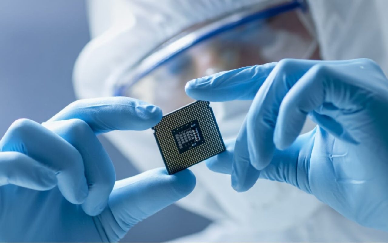
Whether you call them “microchips,” “computer chips,” or just “chips,” we all know how vital semiconductors are to 21st century life.
“Chips are everywhere – in our phones, our TVs, our cars, our kitchen appliances, our kids’ toys,” says Angela Julien, division vice president and business director, Corning Semiconductor Technologies & Solutions. “And the technology behind them continues to push the limits of what is possible.”
You may be surprised to learn how indispensable Corning technology is to this essential industry.
“Without our components, you simply could not produce semiconductors,” says Greg Arserio, division engineering director for Corning’s Advanced Optics business. “There are very few companies in the world that make the machines to produce chips, and Corning is one of their major suppliers. It’s a source of pride.”
For more than 50 years, Corning teams have met ever-increasing challenges to help industry leaders produce tinier and more powerful chips deployed in more products than ever.
How Does Corning Contribute?
Corning supplies materials and components in the production systems that are central to nearly every step of the semiconductor chip manufacturing process.
Corning’s Role in Semiconductor Production
Chips come in a mind-boggling array of types suited to specific uses. Each design requires precise manufacturing processes that can vary accordingly. Corning assists with many of them, in all their complexity.
So, for the purposes of this overview, we’ve simplified and summarized the types of products Corning provides to help our customers make chips. For more detailed information about our semiconductor technologies and solutions, please click the links.
What We Make: Vital Components for Chip Manufacturing

Polysilicon Manufacturing for Wafers:
Wafers serve as the base upon which integrated circuits are built. Our majority-owned subsidiary Hemlock Semiconductor (HSC) makes hyper-pure polysilicon, the raw material used to create silicon wafers deployed in electronic devices. In fact, silicon is the “semiconductor” in a semiconductor device.
Metrology/Inspection:
Wafers must maintain perfect flatness throughout the semiconductor manufacturing process. Corning’s advanced metrology instruments precisely measure flatness and other dimensional characteristics critical to yield.
During different manufacturing steps (and often multiple cycles within each step), Corning precision optical assemblies enable inspection of incredibly small features, looking for potential defects at sub-micron levels—helping ensure the highest-quality end-product.

Photolithography:
Photolithography is the process of directing light to form a circuit’s intricate design on a wafer. Corning helps enable this crucial step for deep ultraviolet (DUV) and extreme ultraviolet (EUV) lithography. Manufacturers use DUV or EUV to create advanced chips for applications like mobile consumer electronics, artificial intelligence, and high-performance computing.
Corning laser optics help enable the generation of intense, stable light for photolithography.
Projection mirrors (for EUV) or lenses (for DUV) made from Corning specialized optical materials then focus the light as it journeys from a patterned photomask.
The photomask acts like a stencil or blueprint for the light to form a circuit’s design on the wafer. EUV photomasks made from Corning® ULE® Glass (Ultra-Low Expansion Glass) help enable accurate pattern-printing. Corning's metrology instruments measure the photomask blank’s flatness and other dimensional factors before the manufacturer gives the photomask its specific circuit design.
In photolithography, nanometers count. With EUV lithography, manufacturers can create chip features 20,000 times smaller than the thickness of a human hair.
There’s no room for error when working at this scale. Corning® ULE® Glass materials provide consistent dimensional stability under a wide range of temperatures and varying conditions during the manufacturing process.
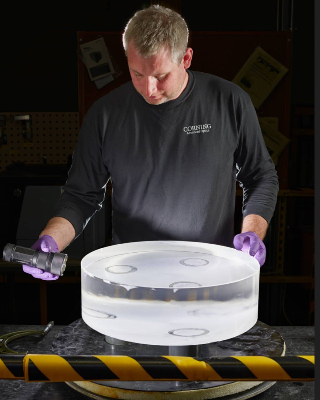 Corning’s experts in Canton, New York, produce Corning® HPFS® Fused Silica. ©Christopher Payne/Esto
Etching:
The etching process carves away unnecessary material to ensure only the imprinted pattern remains. Manufacturers use etching rings made from Corning® HPFS® Fused Silica. This glass substrate’s extreme purity helps minimize potential defects.
Packaging & Glass Wafers:
During packaging, a chip/semiconductor wafer must be properly handled and supported to connect seamlessly to other elements like integrated circuit substrates.
Manufacturers often must thin the wafer at this stage using various methods like grinding and polishing. Corning glass carrier solutions serve as a stabilizing layer under the semiconductor wafer, helping to prevent warp and other damage during these thinning processes. Corning also supplies glass-based temporary bonding solutions for advanced semiconductor packaging processes such as fan-out, 2D, and 3D packaging.
For wafers, an evolution of the semiconductor manufacturing process requires micro-level optic features on the glass wafer. Corning’s products support this advancement in how we deliver next-gen capability.
Evolving For Growth
As companies and governments invest in creating resilient semiconductor supply chains, Corning remains the industry’s reliable resource for fueling growth through innovation.
“We have a lot of responsibility there,” Arserio says. “Our teams are inherently technically curious. And having the capability to continuously learn with this evolving industry puts Corning in a unique position. There’s a reason not everyone can jump to meet this demand.”
“We are manipulators of light,” adds Charles Phillip, Corning’s business application manager for Lithography. “We bend it, we shape it, we use it to pick up information. We drill and cut with light. And we make our own materials to do this. So, as technology gets smarter and smaller, imagine us as the masters of light behind it all.”